EECS 140 ALU
Arithmetic Logic Unit
Contents
Objectives
The objective of this laboratory is to apply knowledge of combinational logic designs to real world application by implementing an arithmetic logic unit into a field programmable gate array chip which can do multiplication (honors only), addition, AND, OR and XOR operations.
Discussion
For this lab, you will use the Flex chip with predefined pin assignments on the Altera UP2 development board. The concept is to design and implement an arithmetic logic unit, which will have the ability to take two four bit binary numbers and depending on a two bit selector either multiply, add, logic AND, or logic OR the two inputs for a five bit binary output. You will use two seven-segment displays to display the binary output in hexadecimal format. Your inputs will range from the hexadecimal numbers 0 to F. Likewise, your outputs will range from 0 to 1E.
In this lab you would be inserting the multiplier and the ripple carry adder design from your previous lab and the 7-segment display unit with altered equations to display hexadecimal numbers. The code for the other components of the ALU is given to you below.
Make sure you design your ALU component with the inputs and outputs of your existing components (multiplier, adder, display) in mind.
Files
ANDer.vhd 4-bit And-gate
ORer.vhd 4-bit OR gate
XORer.vhd 4-bit XOR gate
MUXer.vhd 4-bit Multiplexer gate
Hex_to_LED.vhd Hexadecimal to 7-segment LED decoder (in case your version has problems)
Mutltiplexer.vhd Multiplexer (version with carry bit output)
Tasks
Quiz
Please answer the following questions and submit to your TA at the start of the lab:
- (Research on your own) What two different sets of operations can an ALU do?
- (Research on your own) What’s the best use for an ALU inside a CPU pipeline: Instruction Fetch (IF), Instruction Decode (ID), Execute (EX), Memory Access (MEM), or Memory Write Back (WB)?
- (Current Lab) Which operations are we to program in our ALU?
- What previously implemented components are we using to create our ALU?
- A bitwise operator affects each pair of significant bits in the operands. The bitwise OR operation result for decimals 610 (01102) OR 510 (01012) is 710 (01112). What is the bitwise AND operation result for decimals 510 AND 910?
Step 1: Pre-Lab
You need to come to class with your design basics prepared. You should have a good idea of the design concept as well as some basic VHDL. In this lab the honors students will create an ALU that implements AND, OR, MULTIPLY, and ADD functions. Everyone else will create an ALU that implements AND, OR, XOR, and ADD functions. Create a block diagram of your top level entity showing all the required ports and components.
Step 2
Once your block diagram is ready think of a method that can possibly reduce the number of gates, like using ripple carry adders in place of several full adders perhaps? Also identify parts of the block diagram of multiplier will make up the entity, which the components, and finally the signals. You will be merging this along with the adder to the ALU template.
Step 3
Write VHDL code for your circuit in Quartus II. Follow the structural/modular method of programming. Be very careful in mapping ports when doing component instantiation. Once the multiplier is done you'd need to simulate it to check whether it is outputting the right values. Once this is done you will download and study the ALU template for the next lab.
Step 4
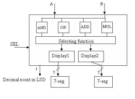
An ALU makes use of multiplexers to route the select the correct answer for its output. You need to create the toplevel entity for your ALU. As always map out your inputs and outputs, signals, components and code in VHDL. Make sure you match cases when specifying names for input and output pins in the module definition and the body of the module. Also make sure all of your outputs are assigned a value at some point. Verify that the left hand side of any assignment is an output.
Step 5
Once you have written your VHDL description of how the circuit should behave you should save and simulate. Compile and simulate each component individually at first.Check the waveform against what the value of a given function should be. If you have errors that need to be debugged, use the simulator to determine which outputs are not working correctly. Look at the output waveform and compare it to the truth tables for 7-segment output. Trace your design and fix any description errors. Consult your T.A. if needed.
Step 6
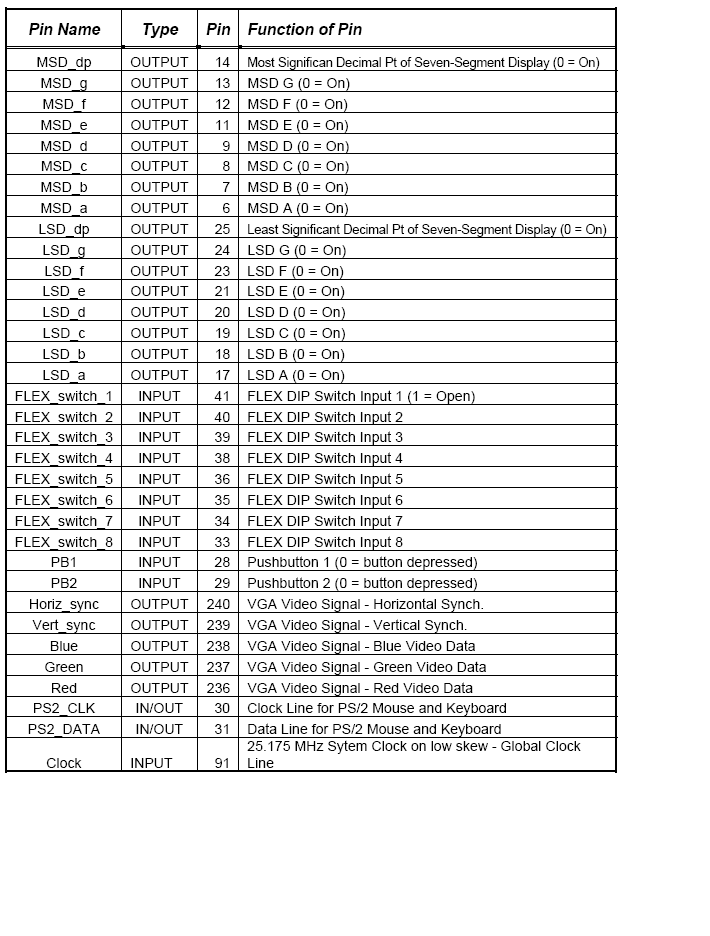
If your circuit simulates correctly then you can assign pins as you did in previous labs. Use the pin assignment table in Figure 1
Step 6
You will program the board as you did in the first laboratory exercise. Go the Quartus II programmer and make sure the board is correctly powered and the Byte Blaster parallel cable is properly connected to the PC you are using.
Select “Programmer” from the list of tools under the Quartus II Menu. Click the Configure button in the programmer window and the circuit should download correctly to the board. If you have any troubles consult your TA.
Step 7
Now you will want to verify that the board is operating correctly. Change inputs using the dip switch and make sure that you get the correct corresponding output. Use the mechanism you selected on the board to select operations (adding, AND, OR). If you get incorrect outputs retrace you steps making sure you have correct pin assignments and that your VHDL is correct or ask your TA. After you’ve tested circuit for proper operation including the overflow detection, show your TA.
Lab Report
Now write your lab report according the format your TA has outlined for you. Make sure to include into your lab report any possibilities of improvements to your circuits or ways you believe it could have been implemented better.