EECS 140 Scrolling Display
Scrolling 7-Segment Display Output
Contents
Objectives
The objective of this laboratory exercise is for you to learn how to use modular design in VHDL to display a scrolling phrase in the visual outputs of the FPGA.
You will use Altera’s Max+plus II software to implement the 7-segment output equations from your PLD lab in VHDL. Using the FLEX chip on the Altera UP2 board, you will download your circuit design to the board and will test proper functionality of the circuit. A 4-bit counter will be provided to you. You are responsible for creating a display driver that interfaces with the counter, and drives the corresponding seven output signals. These signals are finally connected to the boards seven segment display pins.
Discussion
For this lab, we will be using a typical form of output in digital logic called a seven segment display.
A seven segment display is composed of seven individual light emitting diodes denoted by the letters A through G as in Figure 1:
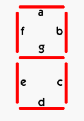
Typically, a seven segment display is a very simple way to output decimal numbers. It can, however, also be used to display hexadecimal and some alphanumeric characters, as you have found out. The phrase (and boolean equations) from your PLD lab will be reused in your display driver, as will the reset logic if you were displaying less than 16 characters. In a similar fashion as in the PLD lab, the 4-bit counter design will provide a repeating series of 0-15 binary number to be used as the inputs to your display driver. In addition, the counter also has extra inputs: Clock, Enable, Initial_Value, Clear_n, and Load_n.
We will also introduce modular design for VHDL. This is a powerful tool to streamline FPGA design, avoid code repetition and enhance portability, reusability and abstraction.
Week 1
Quiz
Please answer the following questions and submit to your TA at the start of the lab:
- A negative logic AND gate is equivalent to what in positive logic?
- (Current Lab) What components will be used in completing this lab?
- How many connections (signals) will connect the counter with the display driver?
- How will we test the result of this lab?
- Suppose you are given a 100-MHz signal how will you generate a 50-MHz and 25-MHz clock signal?
VHDL Tutorials
If you haven't done so yet, review the following tutorials for VHDL, FPGAs and Altera Quartus II. Pay special attention the the modular VHDL tutorial, as from now on we will use modular VHDL almost exclusively.
- This VHDL tutorial will teach about the VHDL language, its fundamentals, and how to represent a simple circuit in VHDL.
- This Modular VHDL tutorial will teach about the using components in VHDL, and creating larger entities by structural design.
- This Altera Quartus II tutorial will teach about using this program to write, simulate, implement and download your circuits into an FPGA. Similar to Exercise 4.
4-bit Counter
Download the above file and take a look at it. Your PCB's 74LS161 four bit counter used frequency division on the clock to achieve counting. How is this VHDL counter different? What is the relationship between the clock's frequency and the counter's (LSB) frequency? Considering the clock in the FPGA oscillates at a rate of 25 MHz, write down as part of your evaluation what the frequency of the oscillator should be. Also include in your lab report how you would alter this file in order to change the counter frequency.
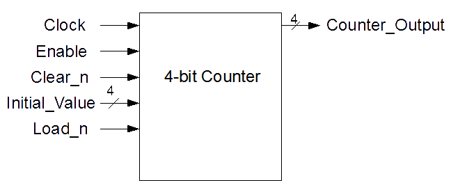
You will quickly learn that you don't need to know how a component works in order to use it in your designs. From the entity description, we know the counter's inputs and outputs:
ENTITY fourbitcounter IS
	PORT
	(
		Clock		: IN	STD_LOGIC;
		Enable		: IN	STD_LOGIC;
		Clear_n		: IN	STD_LOGIC;
		Initial_Value	: IN	STD_LOGIC_VECTOR(3 downto 0);
		Load_n		: IN	STD_LOGIC;
		Counter_Output	: OUT 	STD_LOGIC_VECTOR(3 downto 0)
	);

END fourbitcounter;
Since we are providing the VHDL for it (inside the architecture), here is what the entity does. It has the same functionality as the 161 counter we used:
- The clock input is connected to a square wave oscillating signal from the FPGA board
- If Enable is on (positive logic, On = '1'), the counter increments its value with time
- When Clear_n is '0' (_n = negative logic, On = '0'), the counter resets to zero "0000"
- Initial_Value is a 4-bit signal that contains an initial value to be loaded into the counter
- Load_n (negative logic) loads the Initial_Value input signal into the counter
- Counter_Output is the 4-bit counter output
The best way to know how components will interact with each other in the future is to create a block diagram. The block diagram that corresponds to the entity is depicted in Figure 2
Display_Driver
You will now create an entity that includes your seven segment and reset equations. Write down all the inputs and outputs needed. If you feel comfortable with STD_LOGIC_VECTORs, you could define your inputs/outputs like that, too. If not, define each bit as a STD_LOGIC.
In specific, your display driver should be similar to the block diagram in Figure 4:
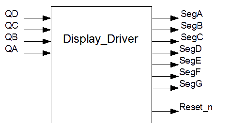
Hence, the entity description for an entity described by the block diagram above would be as follows:
ENTITY display_driver IS
	PORT (
		QD, QC, QB, QA		: IN STD_LOGIC;
		SegA, SegB, SegC, SegD, SegE, SegF, SegG: OUT STD_LOGIC;
		Reset_n: OUT STD_LOGIC);
END display_driver;
Since this a behavioral entity (its outputs can be fully described as a function of the inputs), you can follow the VHDL example in the tutorial book or from Exercise 4 (Negative OR gate) as a skeleton for your entity. Obviously, the number of inputs and outputs, as well as their names, should change to match your entity. For the entity's name, you can choose something like display_driver, pld_to_vhdl, pld_to_fpga, my_display_driver, or similar... just make sure that the file name matches the name of the entity: display_driver.vhd, pld_to_vhdl.vhd, pld_to_fpga.vhd, etc.
Since the outputs (including reset_n) will be connected to negative logic LEDs (or in the case of the reset, a port defined as negative logic), be sure to negate your equations: segA <= NOT( ... );
Compile your design in Max+plus II and correct any errors.
Simulation
Your display driver is not attached to any inputs as of yet. This is an ideal situation to test the correct behavior by simulation. Use the same simulation techniques as in the first FPGA exercise. While in the waveform window, select File->End time and change it from 1.0µs to 1.6µs. This will give you enough space to test for all 16 possible 4-bit combinations.
Your resulting simulation should look like a rotated and inverted (1=>0, 0=>1) version of the original truth table you used.
Counter with display
It is now time to use your fourbitcounter and display_driver entities as components for a new, larger VHDL design. If you are unsure what the difference between entities and components are, be sure to reread the Modular VHDL tutorial.
Step 1: New VHDL entity
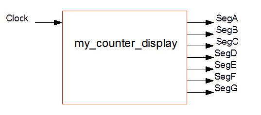
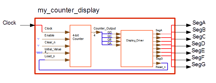
The first step is to create a new file for your new top-level ENTITY. You can call it something like my_counter_display (file name: my_counter_display.vhd). Since this is your top-level design (for this lab), all input and output PORTs will have connections to the FPGA board. Hence, the only input would be a clock signal, and the outputs would be seven signals going to the seven segment display. Hence the block diagram is similar to Figure 5:
Notice that we are color coding the different parts of our design as in the VHDL modular tutorial.
Entity
Component
Signal
Port Mapping
Hence, the entity declared by the bounding red box in the block diagram would be:
ENTITY my_counter_display IS
	PORT (
		Clock		: IN STD_LOGIC;
		SegA, SegB, SegC, SegD, SegE, SegF, SegG: OUT STD_LOGIC);
END my_counter_display;
Step 2: Declare components
Inside the ARCHITECTURE, you need to define which COMPONENTs this entity will use. Not surprisingly, the components will be the fourbitcounter and your display_driver. Declare both of these components:
ARCHITECTURE structural OF my_counter_display IS

-- Component Declaration
COMPONENT fourbitcounter IS
	PORT
	(
		Clock		: IN	STD_LOGIC;
		Enable		: IN	STD_LOGIC;
		Clear_n		: IN	STD_LOGIC;
		Initial_Value	: IN	STD_LOGIC_VECTOR(3 downto 0);
		Load_n		: IN	STD_LOGIC;
		Counter_Output	: OUT 	STD_LOGIC_VECTOR(3 downto 0)
	);

END COMPONENT fourbitcounter;

COMPONENT display_driver IS
	PORT (
		QD, QC, QB, QA		: IN STD_LOGIC;
		SegA, SegB, SegC, SegD, SegE, SegF, SegG: OUT STD_LOGIC;
		Reset_n: OUT STD_LOGIC);
END COMPONENT display_driver;
It should be no surprise that the PORT declarations are exactly the same as when we created their entities. From the block diagrams we previously made, and with the ENTITY description of our final top level module, my_counter_display, a Block diagram of all components and all connections (SIGNALS) between them would look like Figure 6:
Step 3: Declare signals
From the diagram, we can now figure out which SIGNALS we need to declare. Give them appropriate names. Besides any user-defined signals, two useful signals to declare are zero and one (and we assign them the corresponding logic values):
SIGNAL zero, one     : STD_LOGIC;
SIGNAL reset_signal  : STD_LOGIC;
SIGNAL init_val      : STD_LOGIC_VECTOR(3 downto 0);
...
Step 4: Architecture body
BEGIN the architecture body. This is were we instantiate the previously declared components. This is an ideal place to assign a value to signals that have no drivers:
BEGIN -- Architecture

zero <= '0';
one  <= '1';
init_val <= "0000";
Step 5: Instantiate components
Now we instantiate our components. During this week, we instantiate each only once, but we could instantiate multiple copies of the same component without having to work out all the truth tables, Kmaps and simplified equations again. In fact, if someone gave us a component in VHDL, we need not look at the inside workings of it, we just need to know what it does, not how it does it. This is the power of modular design (analogous to abstraction and object oriented programming in software).
Instantiate one copy of the counter, and one copy of your display driver. This means:
- Give it a unique name
- Say which component it is (display_driver, fourbitcounter)
- PORT MAP: For each PORT in the component, specify what signal or entity port it is mapped to. (PORT on the left, MAPPING on the right)
For example, to instantiate one copy of the counter following the example, the code would be with the:
-- Component Instantiation
the_fourbitcounter: fourbitcounter
PORT MAP (
	Clock		=> Clock,
	Initial_Value	=> init_val,
	Clear_n		=> reset_signal,
	Enable		=> one,
	Load_n		=> one,
	Counter_Output	=> four_bit_signal);
where Clock is the only port which is connected to an entity input (also called clock), and all the others are connected to signals (but four_bit_signal hasn't been declared in our sample code).
- Note: you don't need to assign a value if the signal is set somewhere else, like when being connected to a component's output port.
Step 6
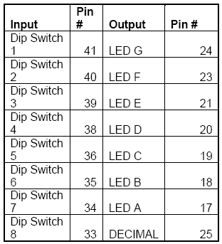
Compile your design in Max+plus II and correct for errors. Once compiled, connect the clock and LED outputs to the correct FPGA pins, listed in Figure 3. The 25MHz clock input comes from Pin 91.
Step 7
Synthesize your design and download it on to the board. You will want to make sure that Max+Plus II has the Flex 10K board with the EPF10K70RC240 chip selected as you did in Lab 4. You can check this by going to the menu Assign -> Device.
Step 8
Test your 7-segment display driver by waiting through all 16 combinations and correcting for errors. Does the correct output appear on the display? Does the display reset correctly at the end of your output? Make sure the equations you entered are correct, and re-synthesize your design.
Week 2
Design modification
We have provided you with most of the VHDL code and block diagrams for a 4-bit counter with display. Modify your design so that you have TWO seven segments running side by side from TWO different counters. While it is true that we could use only one counter, whose outputs would be shared by two seven-segment displays, go ahead and instantiate another counter.
Create separate signals for the Initial_Value, Clear_n and the Counter_Output of this counter. The other ports of the counters can be connected to the same signals (Hence, they're enabled at the same time, they share the same clock, etc).
The new display driver will force you to have 7 more outputs to connect it to. This will require you to modify your entity description.
Design download
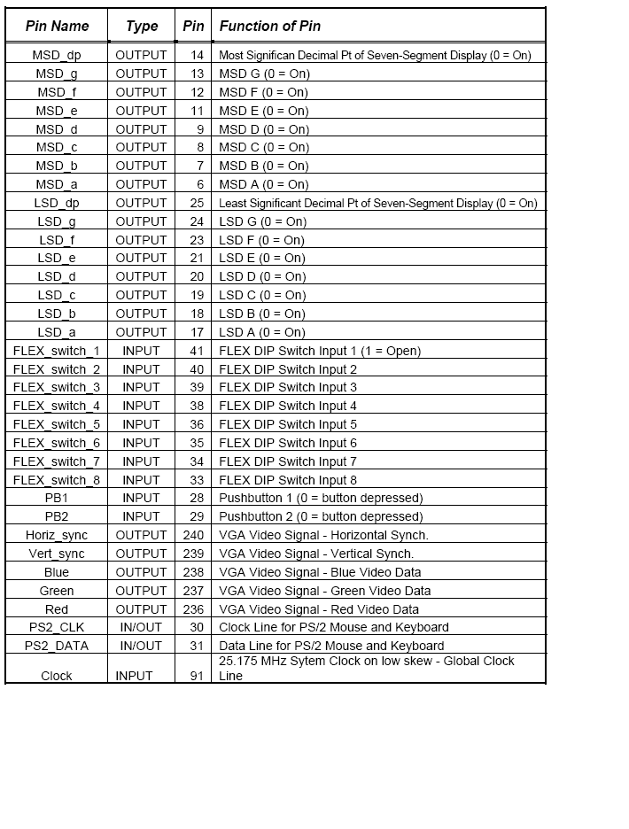
Assign the new seven-segment output pins from the table in Figure 7. "MSD" refers to the seven-segment of the left, "LSD" the one on the right.
Compile, assign pins, and download your new design. You should see your display phrase running side-by-side in the two seven-segment displays.
Scrolling message
- Add an extra input to your entity, since we will have a Load_n input.
- Connect it to the Load_n inputs on both the counters.
- Change the initial_value on the right counter to be "0001". The one on the left should remain "0000"
- Compile your new design
- Assign one of the Push Button pins to the Load_n signal
- Compile again so that the new pin assignment takes place
- Download your program
- Once you hit the Push Button, the counters will load different initial values, but at the same time.
- You should see your design scrolling
Lab Report
Now write your lab report according the format your TA has outlined for you. Make sure to include into your lab report any possibilities of improvements to your circuits or ways you believe it could have been implemented better. Be sure and include all block diagrams, source code and simulator output in your report as well.