EECS 140 Multiplier
Multiplier with Display
Contents
Objectives
The objective of this laboratory exercise is for you to learn how to use modular design in VHDL to create a real world application by implementing a multiplier unit into an FPGA chip and display the multiplication result.
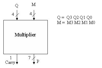
You will use Altera's Quartus software to implement a 4-bit multiplier circuit. You will then connect the result of the multiplier to the inputs of two of your display drivers (from the previous lab). Finally, you will download the circuit design to the board and will test proper functionality of the circuit. An eight bit dip switch will be used for implementing two 4-bit numbers, the multiplication will be outputted on the seven segment LEDs.
Discussion
For this lab, you will use the Flex chip with predefined pin assignments on the Altera UP2 development board. The concept is to design and implement a multiplier, which will have the ability to take two 4-bit binary numbers and output its 8-bit multiplication result. You will use two seven-segment displays to display the binary output in hexadecimal format. Your inputs will range from the hexadecimal numbers 0 to F. Likewise, your outputs will range from 00 to E1.
We will also introduce modular design for VHDL. This is a powerful tool to streamline FPGA design, avoid code repetition and enhance portability, reusability and abstraction.
Files
Template for your 4-bit multiplier Entity multiplier.vhd
Tasks
Quiz
Please answer the following questions and submit to your TA at the start of the lab:
- (Previous Lab) Why did we have to negate the outputs of the seven segment display?
- If we wanted the display to light up the left seven segment LEDs instead of the right ones, what would we change?
- (Current Lab) What's the basic component we will use to implement our 4-bit multiplier?
- Why is modular VHDL important?
- How will we output the result of the multiplication?
Step 1: VHDL Tutorials
If you haven't done so yet, review the following tutorials for VHDL, FPGAs and Quartus. Pay special attention to the modular VHDL tutorial; from now on we will use modular VHDL almost exclusively.
- This VHDL tutorial will teach about the VHDL language, its fundamentals, and how to represent a simple circuit in VHDL.
- This Modular VHDL tutorial will teach about the using components in VHDL, and creating larger entities by structural design.
- This Altera Quartus II tutorial will teach about using this program to write, simulate, implement and download your circuits into an FPGA.
Step 2: Multiplier Design
You should have a good idea of the multiplier design concept as well as some basic VHDL. Given below is the basic operation of a multiplier, which can be implemented using AND gates and Full Adders. Your multiplier should be able to accept two 4-bit numbers and convert it into an 8-bit product. Think of an efficient way to design the multiplier.
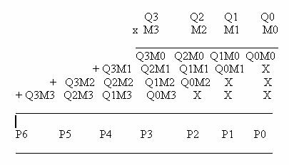
Once your block diagram including all components and signals inside your multiplier is ready, identify which parts will make up the entity, which the components, and finally count all the intermediate signals and give them appropriate names.
Step 3: Structural VHDL
Write VHDL code for your circuit in Quartus. Follow the structural/modular method of programming. Be very careful in mapping ports when doing component instantiation. Once the multiplier is done you'd need to simulate it to check whether it is outputting the right values.
Step 4: Simulation
Once you have written your VHDL description of how the circuit should behave you should save and simulate. Compile and simulate each component individually at first. Check the waveform against what the value of a given function should be. If you have errors that need to be debugged, use the simulator to determine which outputs are not working correctly. Look at the output waveform and compare it to the truth tables for 7-segment output. Trace your design and fix any description errors. Consult your T.A. if needed.
Step 5: Multiplier with Display
Once your circuit simulates correctly, create a new entity 'multiplier_with_display' that will use your multiplier as a component. This new entity will also use your display driver as a component. Declare each component, declare the signals that will connect them, instantiate the components and do a port map to connect them to inputs, outputs or signals. Remember that you will use 2 instances of your display driver to display the 8-bit multiplication result.
Step 6: Download to the Board
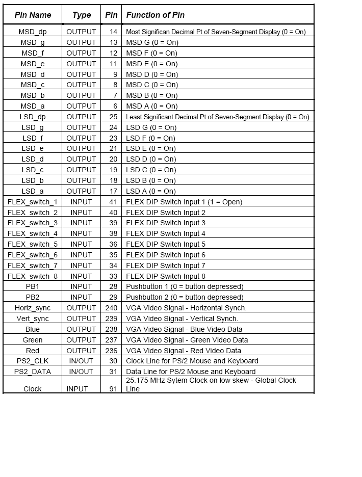
Once your new entity compiles and simulates, assign pins to your entity's inputs and outputs. Use the pin assignment table in Figure 3. You want to assign your multiplier's input Q[3:0] to Flex_Switch[1-4] and input M[3:0] to Flex_Switch[5-8]. Assign the appropriate pins of your display to either the Most Significant Display(MSD) or the Least Significant Display (LSD) seven segment LED pins.
You will program the board as you did in the first laboratory exercise. Go the Quartus programmer and make sure the board is correctly powered and the Byte Blaster parallel cable is properly connected to the PC you are using.
Select "Programmer" from the list of tools under the Quartus Menu. Click the Configure button in the programmer window and the circuit should download correctly to the board. If you have any troubles consult your TA.
Step 7: Evaluate and Correct
Now you will want to verify that the board is operating correctly. Change inputs using the dip switch and make sure that you get the correct corresponding output. If you get incorrect outputs retrace your steps making sure you have correct pin assignments and that your VHDL is correct. After you've tested circuit for proper operation, show it to your TA.
Lab Report
Now write your lab report according the format your TA has outlined for you. Make sure to include into your lab report any possibilities of improvements to your circuits or ways you believe it could have been implemented better.