EECS 140 Seven Segment Display
Seven Segment Display Driver
Contents
Objectives
The objective of this laboratory exercise is for you to use VHDL to create a useful component and implementing it in an FPGA chip.
You will use Altera's Quartus software to implement a generic 7-segment output component, and use it to provide output for a 4-bit input. You will then download the circuit design to the board and will test proper functionality of the circuit. The FPGA board's dip switches will be used for inputting a 4-bit binary number, and the visual representation of that number outputted on the seven segment LEDs.
Discussion
For this lab, you will use the Flex chip with predefined pin assignments on the Altera UP2 development board. The concept is to design and implement a driver with the ability to take a 4-bit binary number and display its value in human readable form. You will use the seven-segment displays to display in hexadecimal format. Your input will range from the hexadecimal numbers 0 to F.
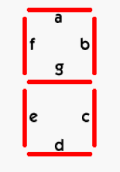
A seven segment display is composed of seven individual light emitting diodes denoted by the letters A through G as in Figure 1:
Typically, a seven segment display is a very simple way to output decimal numbers. It can, however, also be used to display hexadecimal and some alphanumeric characters, as you have found out.
Tasks
Quiz
Please answer the following questions and submit to your TA at the start of the lab:
- (Previous Lab): What was the purpose of the compiler?
- Why are "don’t care" conditions used?
- (Current Lab) Does this seven segment display have any "don't care" conditions? Why or why not?
- A building has 40 floors. The elevator displays the floor number in the decimal system. How many seven segment displays do you need? How many bits to code the floor number?
- Using the example above: Does the seven segment display have any "don't care" conditions? Why or why not?
Step 0: VHDL Tutorials
If you haven't done so yet, review the following tutorials for VHDL, FPGAs and Quartus.
- This VHDL tutorial will teach about the VHDL language, its fundamentals, and how to represent a simple circuit in VHDL.
- This Altera Quartus II tutorial will teach about using this program to write, simulate, implement and download your circuits into an FPGA.
Step 1 : Display Driver
You will now create an entity that includes your seven segment equations. Write down all the inputs and outputs needed. If you feel comfortable with STD_LOGIC_VECTORs, you could define your inputs/outputs like that, too. If not, define each bit as a STD_LOGIC.
Specifically, your display driver should be similar to the block diagram in Figure 4:
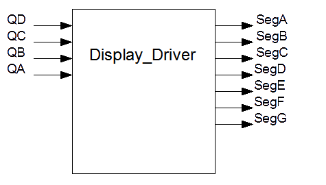
Hence, the entity description for an entity described by the block diagram above would be as follows:
ENTITY display_driver IS
	PORT (
		QD, QC, QB, QA                           : IN STD_LOGIC;
		SegA, SegB, SegC, SegD, SegE, SegF, SegG : OUT STD_LOGIC);
END display_driver;
Since this a behavioral entity (its outputs can be fully described as a function of the inputs), you can follow the VHDL tutorial as a skeleton for your entity. Obviously, the number of inputs and outputs, as well as their names, should change to match your entity. For the entity's name, you can choose something like display_driver... just make sure that the file name matches the name of the entity: display_driver.vhd, seven_segment.vhd, etc.
Step 2 : Truth Table
- Use a truth table to represent all possible states for the 4-bit input
- Draw a column to represent the number/letter you are displaying for a given input. For example, if your input was "1010" (10 in decimal), you would represent this in Hex as "A".
- Draw 7 extra columns to represent all the outputs, SegA through SegG
- Fill in the '1' or '0', depending on if the Segment should be On or Off for the number you are trying to represent. Using the example above, to represent "A", we would need all segment to be lit up, except for the bottom one (SegD). Hence, all outputs for that row (1010) would be '1', except for SegD with a '0'.
Step 3 : Equations
- Now that you have the outputs in the truth table, represent them in minimized SOP (Sum-Of-Products) form
- Type the equations in your VHDL file
- Since the outputs will be connected to negative logic LEDs, be sure to negate your equations:
segA <= NOT( ... );
- Compile your design in Quartus and correct any errors.
Simulation
Your display driver is not attached to any inputs yet. This is an ideal situation to test the correct behavior by simulation. Use the same simulation techniques as in the first FPGA exercise.
Your resulting simulation should look like a rotated and inverted (1=>0, 0=>1) version of the original truth table you used.
Download
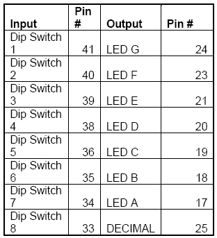
Use the same steps to download your design into the FPGA board. Use 4 dip switches as the 4-bits of input, and the LEDs as the output. The pin assignments are listed below:
Step 7: Evaluate and Correct
Now you will want to verify that the board is operating correctly. Change inputs using the dip switch and make sure that you get the correct corresponding output. If you get incorrect outputs retrace your steps making sure you have correct pin assignments and that your VHDL is correct. After you've tested circuit for proper operation, show it to your TA.
Lab Report
Now write your lab report according the format your TA has outlined for you. Make sure to include into your lab report any possibilities of improvements to your circuits or ways you believe it could have been implemented better.