EECS 140 SOP proto board
From ITTC
Implementing a SOP Expression on Prototyping board
Objectives
Solder IC sockets, bypass capacitors, power and ground buses and interconnections headers.
Pre-lab work:
- What are the three main sections of the prototype board that you soldered in Lab 4.
- How many possible inputs and outputs can you have on the prototype board?
- How would you provide a logic '0' or '1' as input?
- How would you monitor the output(component and logic)?
NOTE: Bring your soldered prototype board along with bag of parts to this lab.
Go to EECS shop on level 3 at Eaton Hall and checkout following items. You must do this before lab start time so consider coming earlier for
the lab.
Digital Probe Kit
Soldering Iron
Safety eyeglass
Wire Cutter
Sponge(Get it slightly wet with few drops of water)
You will need your KUID to checkout these item. Items need to be returned after use.

Location: 3060 Eaton Hall
Instructions Manual
     Detailed Instructions for Soldering: https://people.eecs.ku.edu/~g328v383/lab5_pdf.pdf
     Read below instructions to make final connections and additional components to solder.
NOTE: You need to solder 4 pieces of 5 pin connection header on to the PCB. The 5 pin connection headers are used to make duplicates for
A,B,C,D
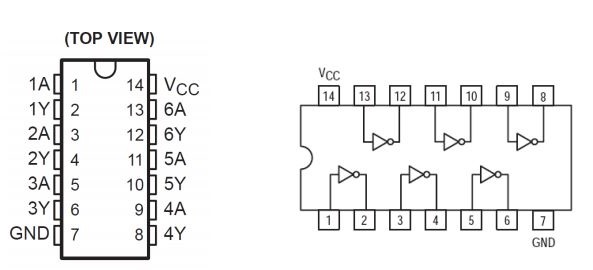
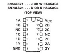
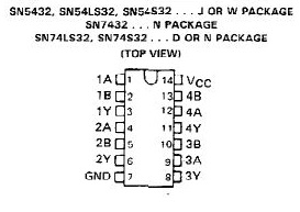
Step1: Vcc and GND has to be connected for each of the ICs to make it work. Pin number 7 is GND and Pin number 14 is Vcc.
You can drive Vcc from 25 pin header next to power diode, while GND from the other 25 pin header.
- SN74LS04N: NOT Gate (Hex Inverters) Partial Datasheet:
Full Datasheet
- SN74LS21: 4 Input AND gate Media:Sn74ls21.pdf:
- SN74LS32: 2 Input OR gates Media:Sn74ls32.pdf:
- Final Connections for the given Boolean Expression:
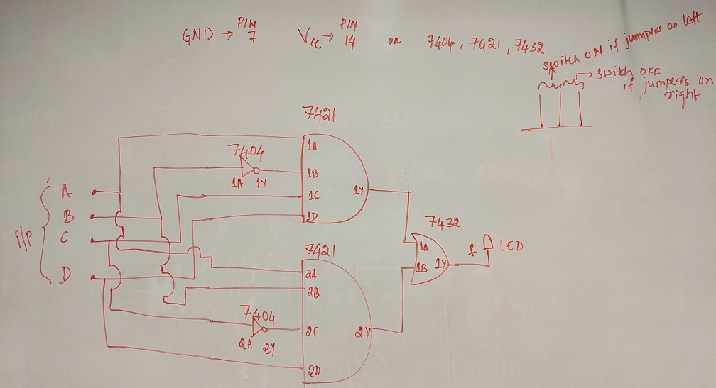
For testing: Write truthtable for boolean expressiong: F = A.B'.C.D + A.B.C'.D
Logic 0 input: Jumper to Right 2 pins of header strip
Logic 1 input: Jumper to Left 2 pins of header strip
Output F-> True/Logic 1/LED OFF
Output F-> False/Logic 0/LED ON
Lab report
Write your lab report as per the instructions by TA.