EECS 140 FPGA Introduction
Introduction to the Altera Flex-10K UP2 Board
Contents
Objectives
The objective of this laboratory is to introduce the student to the Altera Flex-10K UP2 development board by programming a simple combinational logic circuit.
This laboratory will use the Altera Quartus II software to program one of the field programmable logic devices contained on the Flex-10K UP2 development board. For an introduction to the Quartus II software, you should read the Altera Quartus II tutorial. After you have followed the steps to implement the simple circuit in this lab, you will be ready to program the board with more complex digital logic circuits in future labs.
Discussion
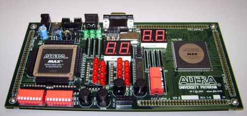
The board being used for this and future labs, the Altera UP2 shown in Figure 1.1, a mid-density FPGA contains the Altera Max 7128 series chip on the left side which has over 2,500 gates well as the FLEX EPF10K70 on the right side has approximately 70,000 gates. This laboratory utilizes the FLEX chip because the pushbuttons and LEDs can be utilized without having to connect the jumper wires that are necessary to use the MAX chip.
This lab will use the two push buttons on the right of the board as well as the seven-segment LED on the right side. Only the decimal point in the middle of the seven segment display connected to pin 14 will be used for output. Both the push buttons and the LED are connected to a pull-up resistor which causes the logic to be "active low." This means that zero volts is tied to the input when the push button is pressed and five volts when it is not pressed. Likewise, the LED requires the FLEX chip to output a low signal to turn on the LED.
The Problem
In order to demonstrate how to program the board in the simplest terms we will build a circuit that utilizes a single gate, the pushbuttons, and the decimal point of the LED. The simple logic equation is as follows:
LED = PB1 + PB2
This is simple, but we must make sure to implement this circuit with active low logic. This can be easily be done by complementing the inputs and outputs of our or gate as follows:
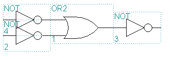
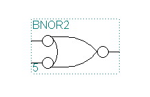
The form shown in Figure 1.2b, known as “negative-logic OR” will be used in the first part of this laboratory.
Tasks
Quiz
Please answer the following questions and submit to your TA at the start of the lab:
- (Previous Lab): How should a good solder joint look like?
- How many different combinations can be generated with 4 bits?
- (Current Lab) What is an FPGA used for?
- What are we doing in the FPGA this lab?
- What kind of logic does the FPGA board use?
Design, Compilation and Simulation
- Create a new folder in drive H: (under "My Computer"), the name of the folder will be your KUID. You will save all your projects here.
- Follow the Altera Quartus II tutorial (Start at step 3).
- Convert your 3-input AND gate (from the tutorial) into a 2-input AND gate, by deleting one of the inputs and modifying the equation. Recompile to make sure there are no mistakes.
- Re-simulate your design which now should only have 2 inputs (and 1 output)
Downloading the Design to the UP2 Board
You must first make sure that the board has been properly connected to the computer and a power source. The AC to DC power transformer plugs into the upper-left input on the board. A 10 pin connector should be plugged into the upper-left portion of the board with the other end being connected to a parallel port on the PC which will be used to program the board with Quartus II.
Now that we’ve made sure the board is properly connected, we need to make sure the jumper settings are set to program the FLEX chip rather than the MAX chip as follows:
The jumpers are located in the upper right hand side of the board, just above the MAX chip.
Assign Device
Quartus will compile differently for different devices (which have different types and numbers of inputs and outputs). To assign the project to the device we have in lab follow these steps:
- In Quartus, Go to the "Assignments" menu and select "Device".
- Under Family chose FLEX10K
- Under available devices, select: EPF10K70RC240-4 (at the bottom)
- Hit OK
- Compile
Assign Pins
Once we have the correct device assigned, it's time to assign pins. By assigning pins, we connect the inputs and output of your design to specific parts of the board. In our case, we want to connect each of your two inputs to a push button, and your output to an LED.
- In Quartus, Go to the "Assignments" menu and select "Pins".
- Make sure there's a table at the bottom of the window. If there is not, select "View", "All pins list" to show it.
- In this table, select one of your inputs. Under "Location", select PIN_28
- Assign your other input's pin. Under "Location", select PIN_29
- Now choose PIN_14 for your output.
- File -> Close
- We need the signals to be routed to their new destination pins. Compile the design to update it.
Download the design to the board
Time to download to the board!
- Choose "Tools", select "Programmer"
- Select your file. It should have the same name as your VHDL entity (.sof extension)
- We need to set the Hardware for Programming. Click on "Hardware Setup"
- Under "Hardware Settings" click on "Add Hardware"
- Select ByteBlaster II and LPT1, and OK
- Double-click on "ByteBlasterII" and make sure it shows up on "Currently Selected Hardware". Close the window.
- Go to "Processing" and "Start" to begin the download.
Test your design by verifying when you push one or both of the push buttons that the un-lit decimal LED lights up. If the LED lights up accordingly you have successfully learned how to program a circuit design on to the board. Otherwise, retrace your steps and make sure you did not commit any errors in your design.
AND gate vs OR gate
You programmed an AND gate, but the circuit behaves like an OR gate!!!! This is due to the negative-logic of the FPGA. While you expected your AND gate to behave like this:
- When both of the push buttons are pressed, the LED is lit.
in reality it acts like this:
- When both of the buttons are unpressed, the LED is un-lit.
This has a duality effect, in which the same behavior can be described with an OR gate:
- When either of the buttons is pressed, the LED is lit.
You will see in lecture how to go from positive to negative logic, using DeMorgan's theorem. In the meantime, remember that the same behavior can be described in different ways.
Lab Report
Write your lab report according the Lab Report Format your TA has provided. Print out your source code (VHDL), and simulation (waveform), and include them in your lab report due next week.