EECS 140 Latches FlipFlops1
Latches, Flip-flops, and Registers
Contents
Objective
The objective of this laboratory is to to investigate latches, flip-flops, and registers.
Discussion
- Latches are circuits that store single bits. One basic type of latch is the RS-latch which has two inputs, labeled Set and Reset. These two inputs, which are typically labeled S and R, provide a means for changing the state, Q, of the circuit. When both inputs, R and S, are equal to 0 the latch maintains its existing state. When R=0 and S=1 the latch is said to be in the Set state. In this case, the circuit output is 1. When R=1 and S=0 the latch is said to be in the reset state and the circuit output is 0. Finally, if R=S=1 the circuit output is going to be 0. This is considered to be an illegal state for an RS-latch.
- A flip-flop is a basic sequential circuit element that stores one bit. A flip-flop changes its output state at the edge of a controlling clock signal.
- When a set of n flip-flops is used to store n bits of information, we refer to these flip-flops as a register. A common clock is used for each flip-flop in a register.
Tasks
Pre Lab
Please answer the following questions and submit to your TA at the start of the lab:
- What is the purpose of a latch?
- How many flip-flops are required to implement a 16 bit register?
- What is the purpose of the VHDL ATTRIBUTE statement in the code snippet shown?
- How will we test the functionality of the gated D latch in this lab?
- Suppose you are given a 100-MHz signal how will you generate a 50-MHz and 25-MHz clock signal?
Step 1: Pre-Lab (Example)
Xilinx FPGAs include flip-flops that are available for implementing a user’s circuit. Later we will show how to make use of these flip-flops. First, we will show how storage elements can be created in an FPGA without using its dedicated flip-flops.

Figure 1 depicts a gated RS latch circuit. A style of VHDL code that uses logic expressions to describe this
circuit is given in the code snippet below. If this latch is implemented in an FPGA that has 4-input lookup tables (LUTs), then
only one lookup table is needed, as shown in Figure 2a.
-- A gated RS latch described the hard way
LIBRARY ieee;
USE ieee.std_logic_1164.all;

ENTITY RSLatch IS
    PORT ( Clk, R, S : IN STD_LOGIC;
           Q         : OUT STD_LOGIC);
END RSLatch ;

ARCHITECTURE Structural OF RSLatch IS
  SIGNAL R_g, S_g, Qa, Qb : STD_LOGIC ;
  ATTRIBUTE keep : boolean;
  ATTRIBUTE keep of R_g, S_g, Qa, Qb : SIGNAL IS true;
BEGIN
  R_g <= R AND Clk;
  S_g <= S AND Clk;
  Qa <= NOT (R_g OR Qb);
  Qb <= NOT (S_g OR Qa);
  Q <= Qa;
END Structural;

Although the latch can be correctly realized in one 4-input LUT, this implementation does not allow its internal signals, such as R_g and S_g, to be observed, because they are not provided as outputs from the LUT. To preserve these internal signals in the implemented circuit, it is necessary to include a compiler directive in the code. In the VHDL code above the directive keep is included by using a VHDL ATTRIBUTE statement; it instructs the compiler to use separate logic elements for each of the signals R_g, S_g, Qa, and Qb. Compiling the code produces the circuit with four 4-LUTs depicted in Figure 2b.

Step 2:
Create a new Vivado project for the RS latch circuit as follows:
- Create a new project for the RS latch on your H:// drive.
- Generate a VHDL file with the code shown above and include it in the project.
- Add a testbench source file to the project. See below for RSLatch testbench
- Run simulation
- Click on Zoom Fit icon in simulation results window to view entire result in one screen
--Add following code for testbench:
--Note: This testbench code is for RSLatch, you need to create testbench codes for DLatch and Master-Slave flip-flop in similar fashion.
LIBRARY ieee;
USE ieee.std_logic_1164.ALL;

ENTITY RSLatch_tb IS
END RSLatch_tb;

ARCHITECTURE behavior OF RSLatch_tb IS

COMPONENT RSLatch
       PORT(Clk,R,S : IN STD_LOGIC;
                  Q : OUT STD_LOGIC);
END COMPONENT RSLatch;

signal S : std_logic := '0';
signal R : std_logic := '0';
signal Clk : std_logic := '0';
signal Q : std_logic;

constant clk_period : time := 10 ns;

BEGIN

uut: RSLatch PORT MAP (Clk => Clk,
                           R=>R,
                           S=>S,
                           Q=>Q);

-- Clock process definitions( clock with 50% duty cycle is generated here.
clk_process :process
  begin
   clk <= '0';
   wait for clk_period/2;
   clk <= '1';
   wait for clk_period/2;
  end process;

rslatch_proc :process
  begin
 s <= '0';
 r <= '1';
 wait for 20ns;
 s <= '1';
 r <= '0';
 wait for 20ns;
 s <= '0';
 r <= '0';
 wait for 20ns;
 s <= '1';
 r <= '1';
 wait for 20ns;
  end process;
END;
Step 3: Gated D Latch (Pay attention to gates used here)
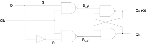
Fig. 3 shows the circuit for a gated D latch. We will implement this latch on the Basys3 board by performing the following steps:
1. Download the correction file below (Right click->Save link as). Also change the file extension from .txt to .tcl
 (Google how to change file extension)
2. Create a new Vivado project. Generate a VHDL file using the style of code shown in Step 1 for the gated D latch. Use the keep directive to
ensure that separate logic elements are used to implement the signals R, S_g, R_g, Qa, and Qb.
3. Goto Bitstream Settings (Right click on "generate bitstream"). Upload Correction.tcl script file onto tcl.pre to avoid any timing errors
4. Compile the code.
5. Verify that the latch works properly for all input conditions
6. Implement the gated D latch on the Basys3 board. Use two slide switches to provide for the inputs D and CLK. DO NOT use 450MHz clock
  signal in constraints file. Look at the output Q on an LED. You would need to write your own XDC file for implementing the D-latch on the
  Basys3 board.
7. Test the functionality of your circuit by toggling the D and Clk switches and observing the Q output.
XDC File Basys3_Constraints

correction correction
NOTE: Gated D-Latch above has different gates than RS-Latch in the example.
Step 4:

Fig. 4 shows the circuit for a master-slave D flip-flop. We will implement this circuit by performing the following steps:
- Create a new Vivado project. Generate a VHDL file (structural model) that instantiates two copies of your gated D latch entity from Step 2 to implement the master-slave flip-flop.
- Include in your project the appropriate input and output ports for the Basys3 board. Use a switch to drive the D input of the flip-flop, and use another switch as the Clock input. Connect the Q output to an LED as discussed in Step 2.
- Compile your project.
- Download the circuit onto the Basys3 board and test its functionality by toggling the D and Clock switches and observing the Q output.
Lab Report
Now write your lab report according the format outlined by your TA. Your lab report should include any suggestions of improvements or ways you believe this lab exercise could have been implemented better.
Acknowledgment
Portions of this lab exercise were put together using material from Altera corporation.