EECS 140 Latches FlipFlops
Latches, Flip-flops, and Registers
Contents
Objective
The objective of this laboratory is to to investigate latches, flip-flops, and registers.
Discussion
- Latches are circuits that store single bits. One basic type of latch is the RS-latch which has two inputs, labeled Set and Reset. These two inputs, which are typically labeled S and R, provide a means for changing the state, Q, of the circuit. When both inputs, R and S, are equal to 0 the latch maintains its existing state. When R=0 and S=1 the latch is said to be in the Set state. In this case, the circuit output is 1. When R=1 and S=0 the latch is said to be in the reset state and the circuit output is 0. Finally, if R=S=1 the circuit output is going to be 0. This is considered to be an illegal state for an RS-latch.
- A flip-flop is a basic sequential circuit element that stores one bit. A flip-flop changes its output state at the edge of a controlling clock signal.
- When a set of n flip-flops is used to store n bits of information, we refer to these flip-flops as a register. A common clock is used for each flip-flop in a register.
Tasks
Quiz
Please answer the following questions and submit to your TA at the start of the lab:
- Which operations did you implement on your ALU last week?
- What is the purpose of a latch?
- How many flip-flops are required to implement a 16 bit register?
- What is the purpose of the VHDL ATTRIBUTE statement in the code snippet shown?
- How will we test the functionality of the gated D latch in this lab?
Step 1: Pre-Lab
Altera FPGAs include flip-flops that are available for implementing a user’s circuit. Later we will show how to make use of these flip-flops. First, we will show how storage elements can be created in an FPGA without using its dedicated flip-flops.
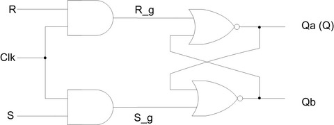
Figure 1 depicts a gated RS latch circuit. A style of VHDL code that uses logic expressions to describe this
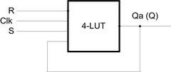
circuit is given in the code snippet below. If this latch is implemented in an FPGA that has 4-input lookup tables (LUTs), then
only one lookup table is needed, as shown in Figure 2a.
-- A gated RS latch described the hard way
LIBRARY ieee;
USE ieee.std_logic_1164.all;

ENTITY RSLatch IS
    PORT ( Clk, R, S : IN STD_LOGIC;
           Q         : OUT STD_LOGIC);
END RSLatch ;

ARCHITECTURE Structural OF RSLatch IS
  SIGNAL R_g, S_g, Qa, Qb : STD_LOGIC ;
  ATTRIBUTE keep : boolean;
  ATTRIBUTE keep of R_g, S_g, Qa, Qb : SIGNAL IS true;
BEGIN
  R_g <= R AND Clk;
  S_g <= S AND Clk;
  Qa <= NOT (R_g OR Qb);
  Qb <= NOT (S_g OR Qa);
  Q <= Qa;
END Structural;
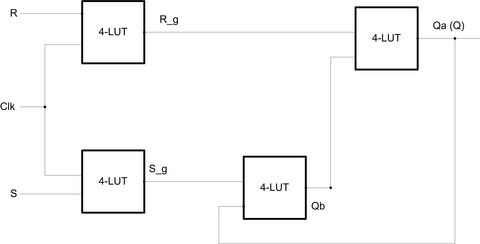
Although the latch can be correctly realized in one 4-input LUT, this implementation does not allow its internal signals, such as R_g and S_g, to be observed, because they are not provided as outputs from the LUT. To preserve these internal signals in the implemented circuit, it is necessary to include a compiler directive in the code. In the VHDL code above the directive keep is included by using a VHDL ATTRIBUTE statement; it instructs the Quartus II compiler to use separate logic elements for each of the signals R_g, S_g, Qa, and Qb. Compiling the code produces the circuit with four 4-LUTs depicted in Figure 2b.
Step 2:
Create a Quartus II project for the RS latch circuit as follows:
- Create a new project for the RS latch. Select as the target device the EPF10K70RC240-4, which is the FPGA chip on the Altera FLEX10K board.
- Generate a VHDL file with the code shown above and include it in the project.
- Create a VectorWaveform File (.vwf) which specifies the inputs and outputs of the circuit. Draw waveforms for the R and S inputs and use the Quartus II Simulator to produce the corresponding waveforms for R_g, S_g, Qa, and Qb. Verify that the latch works as expected using both functional and timing simulation.
Step 3:
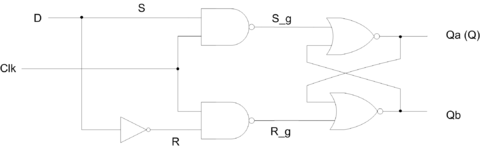
Fig. 3 shows the circuit for a gated D latch. We will implement this latch on the FLEX10K board by performing the following steps:
- Create a new Quartus II project. Generate a VHDL file using the style of code shown in Step 1 for the gated D latch. Use the keep directive to ensure that separate logic elements are used to implement the signals R, S_g, R_g, Qa, and Qb.
- Select as the target chip the FLEX10K EPF10K70RC240-4 and compile the code.
- Verify that the latch works properly for all input conditions by using functional simulation. Examine the timing characteristics of the circuit by using timing simulation.
- Implement the gated D latch on the FLEX10K board. Use a top-level entity that contains the appropriate input and output ports (pins) for the FLEX10K board. Instantiate your latch in this top-level entity. Use PB1 to drive the D input of the latch, and PB2 as the Clk input. Connect the Q output to the decimal point on the least significant digit display. The required pin numbers are: PB1 = PIN_28, PB2 = PIN_29, and dp = PIN_14.
- Recompile your project and download the compiled circuit onto the FLEX10K board.
- Test the functionality of your circuit by toggling the D and Clk switches and observing the Q output.
Step 4:
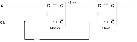
Fig. 4 shows the circuit for a master-slave D flip-flop. We will implement this circuit by performing the following steps:
- Create a new Quartus II project. Generate a VHDL file that instantiates two copies of your gated D latch entity from Step 2 to implement the master-slave flip-flop.
- Include in your project the appropriate input and output ports for the Altera FLEX10K board. Use switch PB1 to drive the D input of the flip-flop, and use PB2 as the Clock input. Connect the Q output to the decimal point of the LSD as discussed in Step 2.
- Compile your project.
- Use the Technology Viewer to examine the D flip-flop circuit, and use simulation to verify its correct operation.
- Download the circuit onto the FLEX10K board and test its functionality by toggling the D and Clock switches and observing the Q output.
Lab Report
Now write your lab report according the format outlined by your TA. Your lab report should include any suggestions of improvements or ways you believe this lab exercise could have been implemented better.
Acknowledgment
Portions of this lab exercise were put together using material from Altera corporation.